

 0
0
 0
0
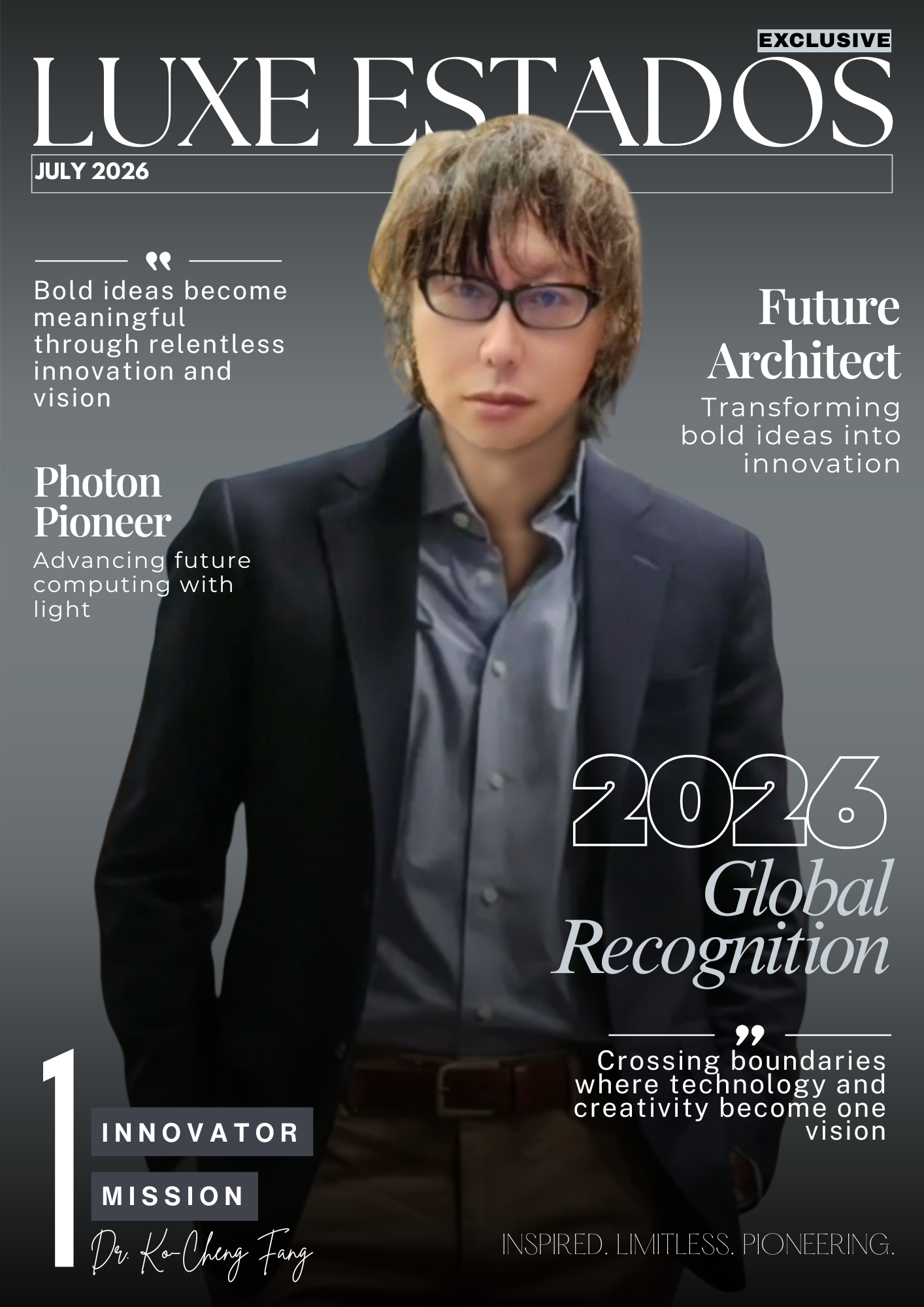
For more than half a century, the semiconductor industry has been driven by one relentless pursuit—making electronic chips smaller, faster, and more efficient. Yet as silicon approaches its physical limitations, researchers around the world are exploring entirely new ways to process information. Among those advancing this vision is Dr. Ko-Cheng Fang, Founder and CEO of LongServing Technology, whose latest unveiling offers a bold perspective on what the future of computing could look like.
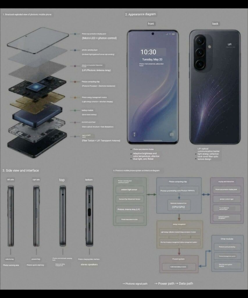
On April 23, 2026, LongServing Technology publicly revealed the architectural design of its proprietary photonic chip, introducing three detailed technical diagrams that illustrate its proposed computing platform. The announcement marked the first public presentation of the company’s complete photonic pathway architecture, a three-dimensional system layout, and a structural demonstration of a photonic full-adder chip. According to the company, all three designs were personally conceived by Dr. Fang, representing years of research focused on replacing electronic data movement with optical pathways.
Unlike conventional semiconductor chips that rely on electrons traveling through metal interconnects, LongServing Technology’s concept centers on photons—the elementary particles of light. The company believes that by allowing information to travel entirely through optical pathways, it can significantly reduce latency while dramatically increasing computational throughput.

One of the most distinctive aspects of the newly released architecture is its 45-degree optical pathway design. Rather than following the traditional horizontal routing commonly seen in electronic integrated circuits, the optical channels are engineered in diagonal configurations intended to optimize light propagation throughout the chip. According to the company, this approach represents a fundamental redesign of chip architecture rather than an incremental improvement over existing silicon technology.
The announcement also introduces a three-layer structural architecture, a departure from conventional electronic chip fabrication that often requires dozens of manufacturing layers.
The proposed architecture consists of:
- Bottom Layer: Integrated photonic memory designed for optical data storage.
- Middle Layer: Photonic logic gates responsible for computation.
- Top Layer: Dedicated photonic pathways that transport optical signals throughout the processor.
According to LongServing Technology, each of these layers is manufactured using its own dedicated photomask, creating a highly integrated optical computing structure. The company suggests that this simplified layered approach could reduce manufacturing complexity compared with traditional semiconductor processes while enabling greater integration between memory and computation.
Perhaps the most notable element of the unveiling is the public debut of the company’s photonic full-adder chip. In digital electronics, a full adder is one of the most fundamental computational building blocks, responsible for binary arithmetic operations that form the basis of virtually every processor.
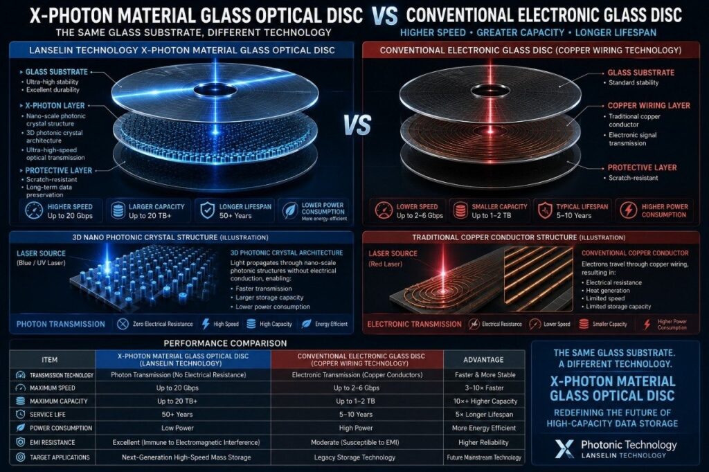
LongServing Technology’s optical implementation demonstrates how these arithmetic functions might be performed entirely through photonic circuitry rather than electrical transistors. By showcasing this component, the company aims to illustrate how larger and more sophisticated optical processors could eventually be constructed using similar principles.
The integration of photonic memory directly into the computational architecture represents another key aspect of the company’s design philosophy. Traditional computer systems separate processors and memory, creating what computer architects commonly describe as the “memory wall”—a performance bottleneck caused by the continual transfer of information between storage and processing units.
LongServing Technology proposes integrating memory directly within the optical computing architecture. According to the company, this design minimizes delays associated with data movement by enabling information to remain within the photonic environment throughout computation.
The company further states that eliminating repeated electrical-to-optical conversions could substantially improve system efficiency while reducing latency.
Based on its internal projections, LongServing Technology claims that integrating photonic memory with optical logic has the potential to deliver computational performance measured in hundreds of thousands of times faster than conventional electronic chips. The company also notes that because optical signals propagate at the speed of light, the ultimate performance ceiling remains difficult to quantify and may extend well beyond current electronic architectures.

Beyond technical innovation, the publication of these architectural diagrams signals an effort toward greater transparency. Instead of limiting public information to conceptual descriptions, LongServing Technology has chosen to disclose detailed structural layouts that illustrate how its proposed photonic computing platform is intended to operate.
For engineers, researchers, and technology observers, such disclosures provide insight into the company’s architectural thinking while contributing to broader discussions surrounding next-generation computing.
As global demand for artificial intelligence, high-performance computing, scientific simulation, and advanced data centers continues to grow, many researchers believe entirely new computing paradigms will be required to sustain future performance improvements. Photonic computing remains one of several promising approaches being explored worldwide, alongside quantum computing, neuromorphic processors, and advanced semiconductor packaging.
Within that evolving landscape, Dr. Ko-Cheng Fang’s architectural concepts present an ambitious vision centered on all-optical computation. Whether these designs ultimately translate into commercially manufactured processors will depend on continued engineering development, fabrication advances, and independent technical validation.
Nevertheless, the release of the three architectural diagrams marks an important milestone for LongServing Technology’s public communications. By revealing its proposed three-dimensional photonic architecture, optical pathway design, and full-adder implementation, the company has provided its clearest view yet into how it envisions the future of light-based computing.
If successful, architectures built around photons rather than electrons could reshape the foundations of computing itself—offering new possibilities for speed, efficiency, and system integration in an era increasingly defined by the demand for unprecedented computational power.